Applied Materials Semiconductor, Flat Panel Display and Solar Photovoltaic Equipment
Applied Materials is the global leader in providing innovative equipment, services and software to enable the manufacture of advanced semiconductor, flat panel display and solar photovoltaic products. Its technologies help make innovations like smartphones, flatscreen TVs and solar panels more affordable and accessible to consumers and businesses around the world. Applied Materials turns today’s innovations into the industries of tomorrow.
Equipment and services for semiconductor, flat panel display and solar photovoltaic product manufacture
Applied Materials is the number one equipment supplier to the semiconductor, liquid crystal display (TFT-LCD) and solar PV industries. It achieved this leadership by focusing on thin film engineering, commercialising sophisticated systems and global reach.
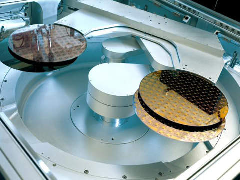
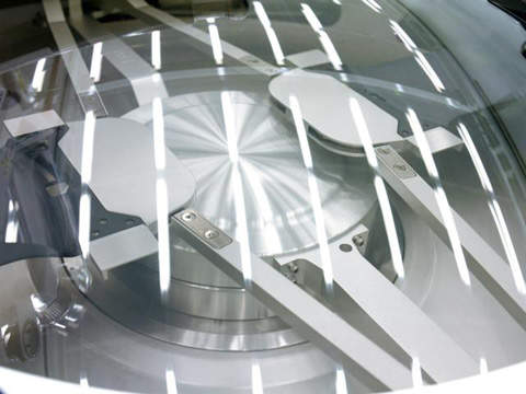
Thin film engineering uses thin films to create electronic structures as small as 1/2,000th the width of a human hair. These films are formed, deposited, shaped and measured by patented Applied Materials processes and tools that provide near-atomic levels of precision and control.
Applied Materials creates sophisticated, commercialised manufacturing systems for ultra-high volume manufacturing and efficiency to drive down the cost of electronic devices. It has a global reach because its intellectual capital, financial resources and capability to help customers integrate and manufacture advanced technology around the world.
Nano manufacturing technology
Applied Materials is the global leader in nano manufacturing technology solutions with a broad portfolio of innovative equipment, service and software products for the fabrication of semiconductor chips, flat panel displays, solar photovoltaic cells, flexible electronics and energy efficient glass.
The company spends approximately $1bn a year on research and development to help ensure process and product leadership. These activities generate many technologies that potentially have applications beyond the domains for which they were developed. Those interested in leveraging these innovations to new areas might benefit by licensing technologies from Applied, possibly resulting in lower product development costs, faster market penetration, and accelerated revenue growth for the licensee.
Applied’s IP portfolio includes more than 8,000 patents worldwide and technologies in the following areas:
- Analytical techniques
- Automation
- Charged particle beams (electron and ion)
- CVD, PVD, ALD, ECP, CMP, RTP and implant
- Etching (conductive and nonconductive)
- Inspection
- Metrology
- Nanotechnology
- Optics (lenses and display)
- Processes (high volume manufacturing (HVM))
- Robots (wafers)
- Thin films including stress engineering
Applied Materials Images

Products and Services
Video
White Papers
Etch Chamber Matching using Applied E3
Etch Chamber Matching using Applied E3
Performance Gains through Automation
Performance Gains through Automation
Predictive Approach Improves Litho Scheduling
Predictive Approach Improves Litho Scheduling
Moving into the Predictive Space with Virtual Metrology
Moving into the Predictive Space with Virtual Metrology
Related Projects
Press Release
Regional Offices
3050 Bowers Avenue
Santa Clara
CA
94052
Other
United States of America