FEI Ultra-High Resolution Tools for Nanoscale Imaging and Analysis
FEI is well-known as one of the world’s premier providers of ultra-high resolution tools for imaging and analysis at the nanoscale. Its tools are used in numerous research and industrial applications worldwide. For the semiconductor industry, FEI tools deliver the data you need, when you need it. As a result, you’ll get to market faster and ramp to volume faster with higher yields. FEI’s solutions are uniquely integrated for the semiconductor lab.
Sub-surface imaging and transmission electron microscopes
A pioneer in sub-surface imaging, it is the leader in DualBeam systems, a technology which it invented. FEI also developed the world’s most powerful, commercially available transmission electron microscope (TEM). Today, FEI offers the broadest range of products, along with ease of use, automation and innovative application support.
FEI delivers superior images, faster sample preparation and more precise circuit editing and analysis, which results in faster design validation and higher throughput process development and control.
Analytic and metrology data
Your equipment investment is safe and secure with stable, long-life solutions that are extensible through several new technology nodes. Your yield and time-to-volume can improve dramatically when you have the finest analytic and metrology data in the shortest possible time. With FEI, you have a partner who is fully committed to helping you get to data faster.
Transmission electron microscope for high quality STEM imaging
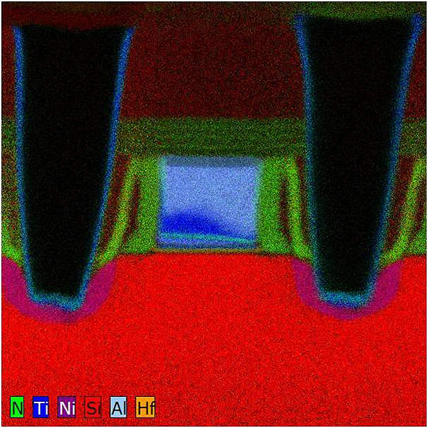
The Tecnai Osiris is a fully digital, high performance 200kV S/TEM system, designed to deliver outstanding performance in all imaging and analytical modes. The combination of a high brightness field emitter and windowless EDX detection using silicon drift detector (SDD) technology lead to unmatched count rates for a given beam current, significantly improved sensitivity for light elements and all in all smart detection of the generated analytical signals.
High output count rates give access to minority element detection since statistically significant peak counts can be collected in viable times. Fast mapping reduces the acquisition time for elemental mappings down to the one for a high quality STEM image turning the grayscale image contrast into color-coded elemental information.
Instruments for 3D microscopy and analysis
The Helios NanoLab 450S is ideally suited for high throughput, high-resolution S/TEM sample preparation, imaging and analysis. Its exclusive FlipStage and in-situ STEM detector can flip from sample preparation to STEM imaging in seconds without breaking vacuum or exposing the sample to the environment.
FEI Images

Products and Services
Video
White Papers
Related Projects
Press Release
Regional Offices
5350 NE Dawson Creek Drive
Hillsboro
Oregon
97124-5793
Other
United States of America
Achtseweg Noord 5, Bldg
5651 GG Eindhoven
Other
Netherlands
NSS-II Bldg 4F
13-34 Kohnan 2-chome
Minato-ku, Tokyo 108-0075
Other
Japan
Unit 102, Building No 8, Micro-electronics Port
No.690 Bibo Road, Pudong
Shanghai 201203, China
Other
China