Trending:
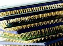
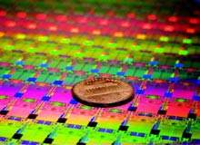
Demand for greater performance from memory and microprocessors is forcing the industry to strive for higher densities. According to AMD's Udo Nothelfer, optical lithography needs innovative technologies and techniques at...
GSF Journal speaks to Bernard Meyerson, the chief technology officer for IBM Systems and Technology Group. He tells us about the company's search for an alternative solution to the problems...
Dragan Boscovic of Motorola, informs Gail Purvis about the continuing evolution of the mobile phone. He tells us what technological advances to expect in the future and how scientists are...
Fostering innovation is essential to continued progress, but it is important to be able to turn ideas into products. Jim Banks speaks to Lisa Su, the senior vice president and...
Gail Purvis presents an exclusive preview of a round-table workshop planned for the Global Semiconductor Forum. She discusses the issue of collaborative innovation with keynote speakers and industry heads.
Michael Garner of Intel answers the crucial questions on emerging research materials (ERM).
Michael Mayberry of Intel tells us about emerging research devices already delivering the goods.
The costs of building and running a semiconductor fab continually on the rise. Joe Draina, the associate director at International SEMATECH Manufacturing Initiative (ISMI), explains how common approaches and solutions...
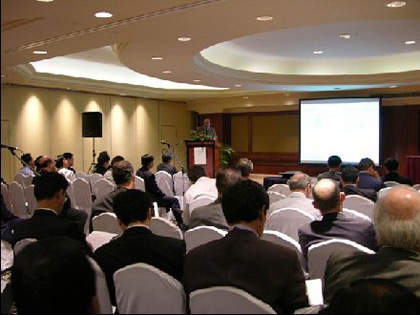
GSF 2006 proved to be the premier event for senior executives within the semiconductor industry. Organised by ViB events, this year's GSF was held at the Shangri-La's Rasa Sentosa Resort,...
Careful patenting of intellectual property is essential if your company is to protect its global interests. Peter Mikhail, Peter Gallagher and James Hsue ask "Are you IP aware?"