Nokia Mobile Phone Production Facility
Nokia has chosen Chennai in the state of Tamil Nadu, Southern India, for its tenth mobile phone factory. The facility wi
Trending:
Nokia has chosen Chennai in the state of Tamil Nadu, Southern India, for its tenth mobile phone factory. The facility wi
Samsung Electronics is constructing a 300mm wafer fab in Austin, Texas. This, the first 300mm...
Read More...
Nokia has chosen Chennai in the state of Tamil Nadu, Southern India, for its tenth...
Read More...
Toshiba Corp. and SanDisk are building a new 300mm wafer fabrication facility at Toshiba's Yokkaichi...
Read More...
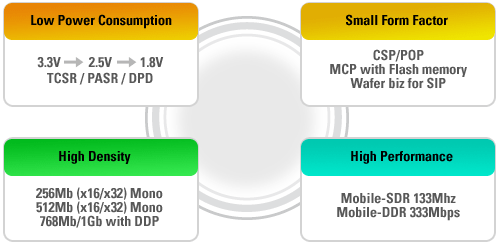
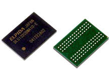
Elpida Memory and Hiroshima Elpida Memory have constructed a second 300mm wafer fab in Hiroshima....
Read More...
AMD’s 300mm 65nm fab in Dresden, Germany, is one of Europe's largest semiconductor manufacturing facilities....
Read More...
Intel’s $2 billion 65nm investment at Leixlip, Ireland, has funded an additional cleanroom at Leixlip...
Read More...
IQE has expanded the range of compound semiconductor materials being produced at its facilities in...
Read More...
Memscap is shipping products from its volume MEMS (micro-electromechanical systems) wafer fab in Bernin, France....
Read More...
Olympus is reorganizing and expanding its Nagano MEMS foundry to produce MEMS on 4in and...
Read More...
TRONIC'S Microsystems is producing 10,000 wafers per year at its MEMS (Micro Electro Mechanical Systems)...
Read More...