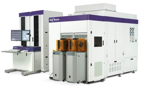
KLA Tencor Process Control and Yield Management for Inspection and Metrology Technologies
KLA-Tencor, a leading provider of process control and yield management solutions, partners with customers around the world to develop state-of-the-art inspection and metrology technologies. These technologies serve the semiconductor, data storage, LED, photovoltaic and other related nanoelectronics industries. With a portfolio of industry-standard products and a team of world-class engineers and scientists, the company has created superior solutions for its customers for over 30 years. Headquartered in Milpitas, California, KLA-Tencor has dedicated customer operations and service centers around the world.
Front-end defect inspection, review and analysis
KLA-Tencor front-end defect inspection tools cover the full range of yield applications within the IC manufacturing environment. This includes incoming wafer qualification, research and development, and tool, process and line monitoring. Patterned and unpatterned wafer defect inspection tools find particles, pattern defects and electrical issues on the front surface, back surface and edge of the wafer. Defect review systems capture high-resolution images of the defects detected by inspectors, enabling defect classification. The defect data generated by inspection and review tools are compiled and reduced to relevant root-cause and yield-analysis information with our suite of data management tools.
By implementing our portfolio of defect inspectors, defect review and classification tools and data management systems, chipmakers are able to quickly identify, monitor and resolve process issues, resulting in higher yield and faster time to market.
Metrology, analysis and process window optimization
KLA-Tencor offers a broad portfolio of metrology solutions that address IC manufacturers’ complex process control measurement challenges. Precise metrology and control of pattern dimensions, film thicknesses, layer-to-layer alignment, pattern placement, surface topography and electro-optical properties are growing in importance as critical dimensions narrow, film thicknesses shrink to countable numbers of atomic layers and devices become more complex.
Whether verifying that a design will be manufacturable, characterizing a new process, or monitoring high-volume manufacturing processes, its comprehensive set of metrology, analysis and process window optimization products gives IC manufacturers the ability to produce high-performance, reliable devices.
Reticle manufacturing and requalification
Error-free reticles, or masks, are the first step in achieving high semiconductor device yields, since reticle defects can be replicated on production wafers. KLA-Tencor offers high sensitivity reticle inspection and metrology systems for mask shops, helping ensure that reticles are defect-free and meet mask metrology requirements. The reticle inspection systems use optical imaging and multiple inspection modes to find all types of reticle defects prior to printing on the wafer.
The metrology systems ensure quality reticle manufacturing by providing the best precision for reticle pattern placement and accurate measurement of reticles’ critical dimensions. Within the IC manufacturing environment, chipmakers rely on its high-sensitivity reticle defect inspection tools to ensure that reticles are defect-free thereby preventing reticle defects from printing on production wafers.
KLA Tencor Images


Products and Services
Video
White Papers
Related Projects
Press Release
Regional Offices
One Technology Drive
Milpitas
95035
California
Other
United States of America