BT Imaging Photo Luminescence Imaging Technology and Equipment
BT Imaging, based in Sydney, Australia, is the photovoltaic (PV) industry’s leading supplier of photo luminescence (PL) imaging technology and equipment.
The technology originates from the world famous Photovoltaic group at the University of New South Wales and and is the result of many years of research and development work by researchers and scientists.
PL technology for the photovoltaic industry
PL technology can be used throughout the whole PV supply chain, from silicon blocks to wafer, cell and modules. It can be used to inspect defects in the silicon material, which have a big impact on solar cell efficiency, and to diagnose solar cell process issues.
As the industry moves to more advanced solar cell technologies, PL will become more important than ever to help achieve and maintain the superior and stable performance of the cell manufacturing line.
Flexible offline characterisation tools for the solar industry
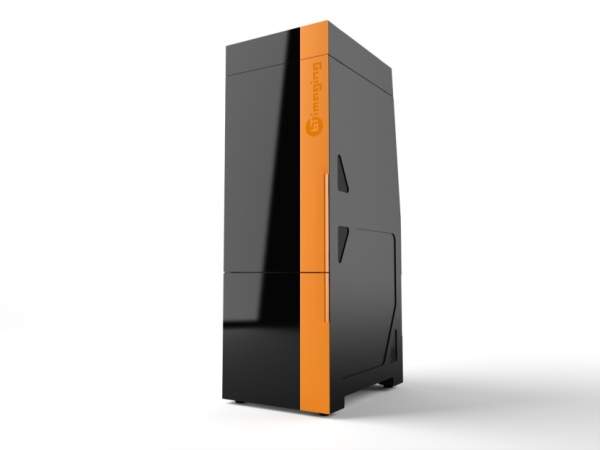
BT Imaging supplies the solar industry with the most comprehensive and flexible offline characterisation tool for R&D purposes, the LIS-R2, which measures silicon blocks, silicon wafers, solar cells and solar modules all within one tool.
It integrates PL, Electroluminescence (EL), series resistance (RS), QSSPC lifetime and calibrated PL measurement; it also uses the second generation PL technology developed by BT Imaging, which can be sped up to more than ten times the original in image acquisition.
It is the fastest PL tool in the world as it takes only two seconds to obtain PL images of as-cut wafers and has the highest resolution capability of 1MP, with a small tool footprint. BT Imaging has the widest installation base, with more than 30 tools used by leading silicon wafer and solar cell manufacturers, equipment vendors and material suppliers.
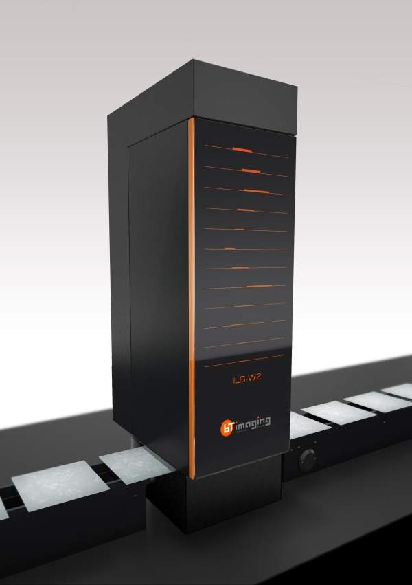
Inline PL technology and equipment for as-cut wafer quality control and yield management
BT Imaging has also developed a third generation of PL imaging optics and technology. These are used in the new iLS-W2 inline tool, which inspects as-cut wafers at 3,600wph with no need to stop the wafer. Full megapixel images are taken ‘on-the-fly’ as the conveyor belt moves wafers under the module.
It is used to sort wafers into different grades based on their defect types and quantities. The tool brings tremendous value to both wafer and cell manufacturers, with clear correlation between wafer defects and cell efficiency. Together, with the inline PL tool, BT Imaging brings yield management and valuable knowledge it has acquired after running hundreds of thousands of wafers and cells.
Wafer quality grading and wafer sorting
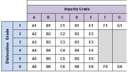
BT Imaging is not only leading the way in new PL inspection tools, but also in image processing and wafer quality grading technologies. Based on a high volume manufacturing experience at leading PV companies, a multi-crystalline wafer quality universal grading system has been developed, in which A1 has low dislocations and no impurity area, while D6 has high dislocations and a high impurity area.
BT Imaging is developing a series of standard recipes that allow manufacturers to bin wafers of different grades into a smaller number of bins. Wafers sorted into physical bins are then used for different purposes.
Use cases currently being evaluated by PV manufacturers include:
- Processing only wafers, which will achieve efficiency above a specific value, e.g. 16.4% or 16.8% depending on their customer’s requirements
- Processing the highest efficiency grade A1 wafers in high efficiency cell processing lines
- Sorting wafers for specific customer orders to manage wafer and cell inventory levels and thus optimise cash flow
- Processing wafers with higher impurity area fraction in cell lines with a higher gettering capability
Cast-mono wafers
Wafer grading based on PL imaging is essential for the new mono-like cast wafer technology. Optically perfect mono-like wafers have a large range of cell efficiency due to dislocations and impurities, as well as the area fraction of the wafer, which is mono crystalline. BT Imaging’s iLS-W2 can quantify all of these critical parameters and grade the wafers.
The grade correlates with the final cell efficiency achieved, so enables PV manufacturers to implement mono-like wafers into production with predictable final performance. Wafer manufacturers can use the PL data both for inline quality control and also to optimise the crystallisation process, with the aim to reduce the density of key defects, such as dislocations, across the ingot.
BT Imaging Images
Products and Services
Video
White Papers
Related Projects
Press Release
Regional Offices
P.O. Box K61
Haymarket
NSW 1240
Australia
1 Blackburn Street
Surry Hills
NSW 2010
Australia